Materials science is a somewhat quiet revolution. Many of the biggest and most valuable inventions have been fueled by materials science innovations over decades. From the foundational computer chip (made from silicon material, of course) to clusters of supercomputers at the Materials Project, research teams are now doing analysis and predictions of how materials can be combined in the most efficient way possible.
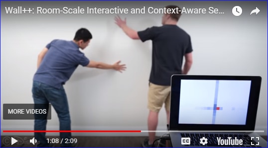
A practical outcome of this sort of advanced materials research is a project between Carnegie Mellon University and Disney Research – that has found a way to change the wall in your home or apartment into a touchscreen interface.
According to the researchers, “the technique involves using water-based nickel conductive paint to create an electrode pattern (a diamond arrangement) suited to capacitive and proximity (electromagnetic) EM sensing. The pattern is then overpainted with latex paint. Each row and column is then connected to a sensor board based on a 96 MHz Cortex M4 running Teensy 3.2 firmware and piped to a laptop for visualization.”
In a nutshell, you could touch the wall to turn on a light – or the electromagnetic sensing would note your presence, your gestures, or your motion to perform an action – much like smart device users are starting to use the Amazon Echo to turn on a light or adjust the air conditioning with a voice command.
Importance to Materials Science Technician Education
The researchers call their system “Wall++” and believe that you could run a light switch or thermostat or other controllers from the wall itself. These materials science research projects are likely to create entire new categories of jobs for people to install, maintain, and service these advanced systems.
For more ideas or direction about advanced materials science technician training in the real world, check out the Nano-Link Regional Center for Nanotechnology Education, a National Science Foundation Advanced Technological Education program, that provides information on nano-tech and nano-materials. One of their industry affiliate partners is the National Nanotechnology Coordinated Infrastructure (NNCI) which lists labs, tools, and experts.
Materials science may not be in the daily news, but it is consistently making headlines. A bright future is ahead for advanced materials and the technicians who want to be part of it.
Resources:
Hat tip to Peter Diamandis, profiled here in the AM News post, Materials Science and Additive Manufacturing Technology Convergence, in one of his recent email newsletters, shared an article link about the Disney Research work. The newsletter summary linked to this article at The Register: Turn that bachelor pad into a touch pad: Now you can paint buttons, sensors on your walls.
Here is the link to the Materials Project site mentioned above.

1 thought on “Disney Research Uses Materials Science To Invent Touchscreen Walls With Conductive Paint”